Wafer (electronics)
Videos
Page
In electronics, a wafer is a thin slice of semiconductor, such as a crystalline silicon, used for the fabrication of integrated circuits and, in photovoltaics, to manufacture solar cells.
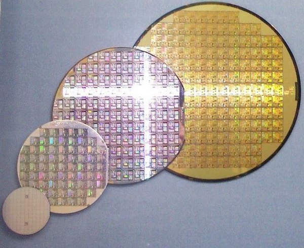
2-inch (51 mm), 4-inch (100 mm), 6-inch (150 mm), and 8-inch (200 mm) wafers
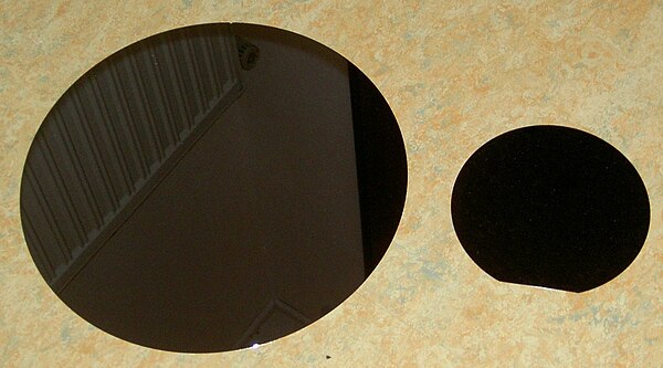
Image: Siliziumwafer

Image: Wafers on the conveyor (3347741252)

Image: Solar World wafer (3347743800)
Semiconductor
Videos
Page
A semiconductor is a material that has an electrical conductivity value falling between that of a conductor, such as copper, and an insulator, such as glass. Its resistivity generally falls as its temperature rises; metals behave in the opposite way. In many cases their conducting properties may be altered in useful ways by introducing impurities ("doping") into the crystal structure. When two differently doped regions exist in the same crystal, a semiconductor junction is created. The behavior of charge carriers, which include electrons, ions, and electron holes, at these junctions is the basis of diodes, transistors, and most modern electronics. Some examples of semiconductors are silicon, germanium, gallium arsenide, and elements near the so-called "metalloid staircase" on the periodic table. After silicon, gallium arsenide is the second-most common semiconductor and is used in laser diodes, solar cells, microwave-frequency integrated circuits, and others. Silicon is a critical element for fabricating most electronic circuits.

An ingot of monocrystalline silicon
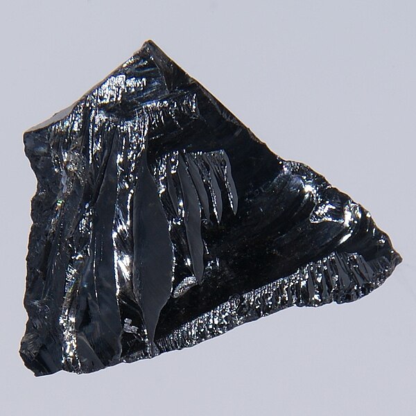
Silicon crystals are the most common semiconducting materials used in microelectronics and photovoltaics.

Karl Ferdinand Braun developed the crystal detector, the first semiconductor device, in 1874.
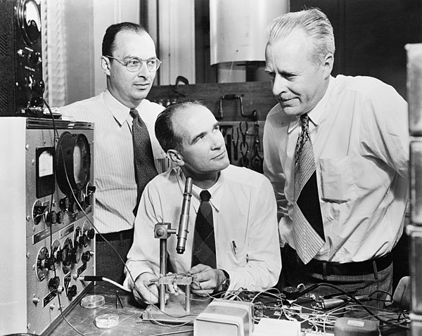
John Bardeen, William Shockley and Walter Brattain developed the bipolar point-contact transistor in 1947.