Laser diode
Videos
Page
A laser diode is a semiconductor device similar to a light-emitting diode in which a diode pumped directly with electrical current can create lasing conditions at the diode's junction.
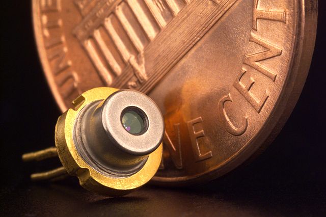
A packaged laser diode shown with a penny for scale*488 nm: InGaN green-blue laser; became widely available in mid-2018.

The laser diode chip removed and placed on the eye of a needle for scale
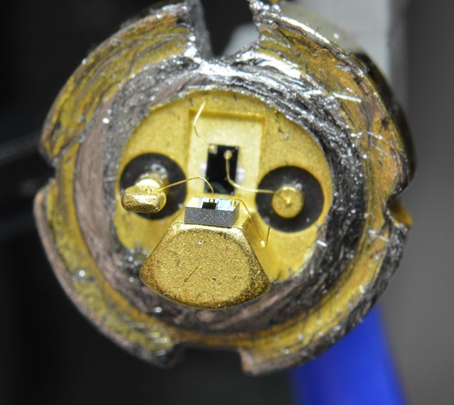
A laser diode with the case cut away. The laser diode chip is the small black chip at the front; a photodiode at the back is used to control output power.

SEM (scanning electron microscope) image of a commercial laser diode with its case and window cut away. The anode connection on the right has been accidentally broken by the case cut process.
Semiconductor
Videos
Page
A semiconductor is a material that has an electrical conductivity value falling between that of a conductor, such as copper, and an insulator, such as glass. Its resistivity generally falls as its temperature rises; metals behave in the opposite way. In many cases their conducting properties may be altered in useful ways by introducing impurities ("doping") into the crystal structure. When two differently doped regions exist in the same crystal, a semiconductor junction is created. The behavior of charge carriers, which include electrons, ions, and electron holes, at these junctions is the basis of diodes, transistors, and most modern electronics. Some examples of semiconductors are silicon, germanium, gallium arsenide, and elements near the so-called "metalloid staircase" on the periodic table. After silicon, gallium arsenide is the second-most common semiconductor and is used in laser diodes, solar cells, microwave-frequency integrated circuits, and others. Silicon is a critical element for fabricating most electronic circuits.
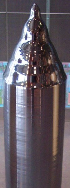
An ingot of monocrystalline silicon
Silicon crystals are the most common semiconducting materials used in microelectronics and photovoltaics.

Karl Ferdinand Braun developed the crystal detector, the first semiconductor device, in 1874.
John Bardeen, William Shockley and Walter Brattain developed the bipolar point-contact transistor in 1947.