The Czochralski method, also Czochralski technique or Czochralski process, is a method of crystal growth used to obtain single crystals of semiconductors, metals, salts and synthetic gemstones. The method is named after Polish scientist Jan Czochralski, who invented the method in 1915 while investigating the crystallization rates of metals. He made this discovery by accident: instead of dipping his pen into his inkwell, he dipped it in molten tin, and drew a tin filament, which later proved to be a single crystal. The method is still used in over 90 percent of all electronics in the world that use semiconductors.
Crystal of Czochralski-grown silicon
Silicon crystal being grown by the Czochralski method at Raytheon, 1956. The induction heating coil is visible, and the end of the crystal is just emerging from the melt. The technician is measuring the temperature with an optical pyrometer. The crystals produced by this early apparatus, used in an early Si plant, were only one inch in diameter.
A puller rod with seed crystal for growing single-crystal silicon by the Czochralski method
Crucibles used in Czochralski method
A crystal is a solid material whose constituent atoms, molecules, or ions are arranged in an orderly repeating pattern extending in all three spatial dimensions. Crystal growth is a major stage of a crystallization process, and consists of the addition of new atoms, ions, or polymer strings into the characteristic arrangement of the crystalline lattice. The growth typically follows an initial stage of either homogeneous or heterogeneous nucleation, unless a "seed" crystal, purposely added to start the growth, was already present.
An example of the cubic crystals typical of the rock-salt structure.
Silver sulfide whiskers growing out of surface-mount resistors.
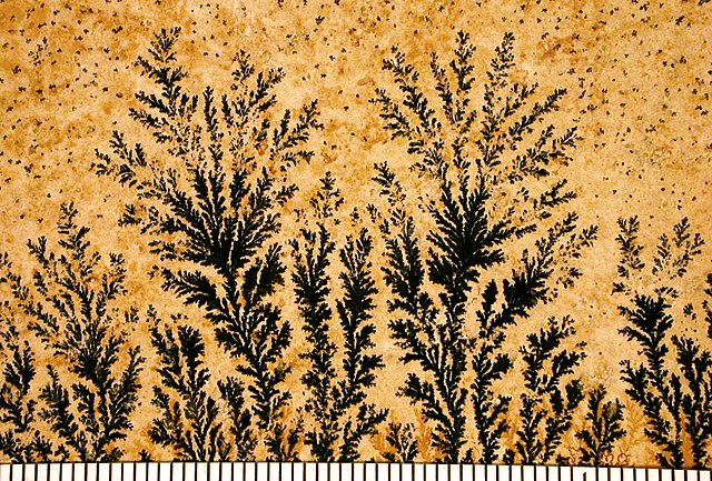
Pyrolusite (manganese(IV) oxides) dendrites on a limestone bedding plane from Solnhofen, Germany. Scale in mm.