Scanning tunneling microscope
A scanning tunneling microscope (STM) is a type of scanning probe microscope used for imaging surfaces at the atomic level. Its development in 1981 earned its inventors, Gerd Binnig and Heinrich Rohrer, then at IBM Zürich, the Nobel Prize in Physics in 1986. STM senses the surface by using an extremely sharp conducting tip that can distinguish features smaller than 0.1 nm with a 0.01 nm (10 pm) depth resolution. This means that individual atoms can routinely be imaged and manipulated. Most scanning tunneling microscopes are built for use in ultra-high vacuum at temperatures approaching absolute zero, but variants exist for studies in air, water and other environments, and for temperatures over 1000 °C.
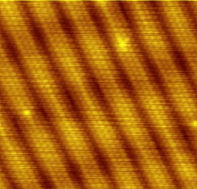
Image of reconstruction on a clean (100) surface of gold
A 1986 STM from the collection of Musée d'histoire des sciences de la Ville de Genève
A large STM setup at the London Centre for Nanotechnology
The characteristic reconstruction fringes on the (100) surface of gold are 1.44 nanometers wide and consist of six atomic rows that sit on top of five rows of the crystal bulk. Image size is approximately 10 nm by 10 nm.
Atoms are the basic particles of the chemical elements. An atom consists of a nucleus of protons and generally neutrons, surrounded by an electromagnetically bound swarm of electrons. The chemical elements are distinguished from each other by the number of protons that are in their atoms. For example, any atom that contains 11 protons is sodium, and any atom that contains 29 protons is copper. Atoms with the same number of protons but a different number of neutrons are called isotopes of the same element.
Scanning tunneling microscope image showing the individual atoms making up this gold (100) surface. The surface atoms deviate from the bulk crystal structure and arrange in columns several atoms wide with pits between them (See surface reconstruction).


