Tunnel diode
Videos
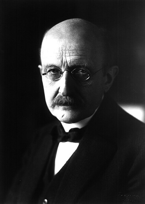
A tunnel diode or Esaki diode is a type of semiconductor diode that has effectively "negative resistance" due to the quantum mechanical effect called tunneling. It was invented in August 1957 by Leo Esaki when working at Tokyo Tsushin Kogyo, now known as Sony. In 1973, Esaki received the Nobel Prize in Physics for experimental demonstration of the electron tunneling effect in semiconductors. Robert Noyce independently devised the idea of a tunnel diode while working for William Shockley, but was discouraged from pursuing it. Tunnel diodes were first manufactured by Sony in 1957, followed by General Electric and other companies from about 1960, and are still made in low volume today.

1N3716 tunnel diode (with 0.1" jumper for scale)

10 mA germanium tunnel diode mounted in test fixture of Tektronix 571 curve tracer

8–12 GHz tunnel diode amplifier, circa 1970

I vs. V curve of 10 mA germanium tunnel diode, taken on a Tektronix model 571 curve tracer.
Quantum mechanics
Videos
Quantum mechanics is a fundamental theory in physics that describes the behavior of nature at and below the scale of atoms. It is the foundation of all quantum physics, which includes quantum chemistry, quantum field theory, quantum technology, and quantum information science.

The 1927 Solvay Conference in Brussels was the fifth world physics conference.