Electron-beam lithography
Videos
Electron-beam lithography is the practice of scanning a focused beam of electrons to draw custom shapes on a surface covered with an electron-sensitive film called a resist. The electron beam changes

An example of Electron-beam lithography setup
A scanning tunneling microscope is a type of scanning probe microscope used for imaging surfaces at the atomic level. Its development in 1981 earned its inventors, Gerd Binnig and Heinrich Rohrer, the
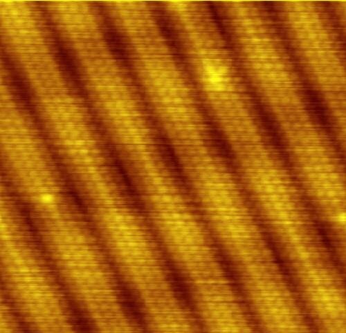
Image of reconstruction on a clean (100) surface of gold

A 1986 STM from the collection of Musée d'histoire des sciences de la Ville de Genève

A large STM setup at the London Centre for Nanotechnology