Extreme ultraviolet lithography
Videos
Page
Extreme ultraviolet lithography is a cutting-edge technology used in the semiconductor industry for manufacturing integrated circuits (ICs). It is a type of photolithography that uses extreme ultraviolet (EUV) light to create intricate patterns on silicon wafers.
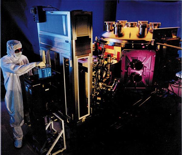
An EUVL tool, Lawrence Livermore National Laboratory
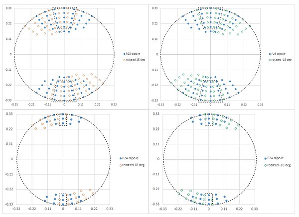
Pupil rotation across slit forces use of much lower pupil fill (within the trapezoids or rectangles) for dipole illumination.
Photolithography
Videos
Page
Photolithography is a process used in the manufacturing of integrated circuits. It involves using light to transfer a pattern onto a substrate, typically a silicon wafer.

The wafer track portion of an aligner that uses 365 nm ultraviolet light