Integrated circuit packaging
Integrated circuit packaging is the final stage of semiconductor device fabrication, in which the die is encapsulated in a supporting case that prevents physical damage and corrosion. The case, known as a "package", supports the electrical contacts which connect the device to a circuit board.
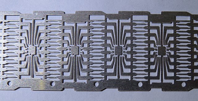
Dual in-line (DIP) integrated circuit metal lead frame tape with contacts
Various IC packages (left to right): TSSOP-32, TQFP-100, SO-20, SO-14, SSOP-28, SSOP-16, SO-8, QFN-28
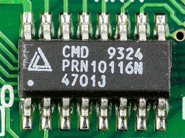
Small-outline integrated circuit. This package has 16 "gull wing" leads protruding from the two long sides and a lead spacing of 0.050 inches.
Early USSR-made integrated circuit. The tiny block of semiconducting material (the "die"), is enclosed inside the round, metallic case (the "package").
Semiconductor device fabrication
Semiconductor device fabrication is the process used to manufacture semiconductor devices, typically integrated circuits (ICs) such as computer processors, microcontrollers, and memory chips. It is a multiple-step photolithographic and physio-chemical process during which electronic circuits are gradually created on a wafer, typically made of pure single-crystal semiconducting material. Silicon is almost always used, but various compound semiconductors are used for specialized applications.
NASA's Glenn Research Center clean room